Shanghai Bontek Optoelectronic Technology Development Co., Ltd
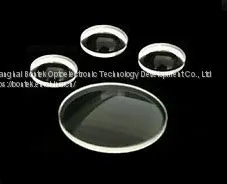
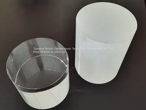
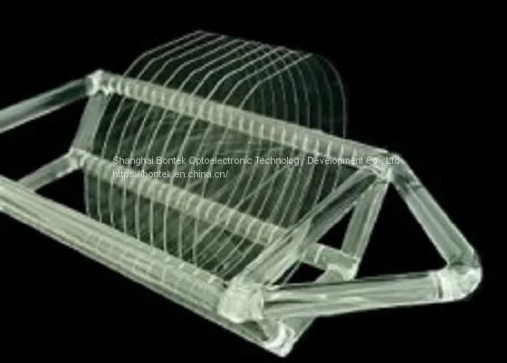
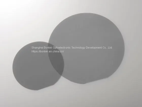
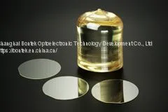
Main Products: Lithium Niobate Wafer, Lithium Tantalate Wafer, Quartz Crystal Wafer, Quartz Crystal Ring, Quartz Crystal Blank, Fused Silica Substrate, Fused Quartz Substrate, Borosilicate Substrate, Fluoride Optical Prism, Fluoride Optical Window, Fluoride Cylindrical Lens, Fluoride Spherical Lens
Home > Company Introduction
Company Overview
Adhering to the development philosophy of specialized research, innovation, openness, and integrity, Shanghai BonTek Optoelectronics Technology Development Co.,Ltd. is deeply involved in the microelectronic materials industry and is a professional optoelectronic material solution provider. We work mostly with wafers, blanks, substrates made from Quartz Crystal, Lithium Niobate, Lithium Tantalate, Fluoride, Glass etc.The company is composed of a group of experienced industry experts and sales consultants, with over 10 years average experience. Relying on a number of shareholding and strategic cooperation factories, BonTek is capable of conducting collaborative research and development with customers. We are committed to providing global customers with high quality microelectronic materials, as well as supporting the construction of 5G network infrastructure and the ecological development of IoT.


-
ManufacturerBusiness Type
-
2020Year Established
-
shanghaiPort of Shipment
-
North America, Eastern Europe, Northern Europe, Southern Europe, Domestic MarketMain Markets

Company Detail
Transparency is the foundation of our partnership. Below is a comprehensive overview of our operational metrics, from business scale to global market reach, giving you a clear picture of our capabilities.
-
21-50 People Sales Staff
-
North America, Eastern Europe, Northern Europe, Southern Europe, Domestic Market Main Markets
-
shanghai Port of Shipment
-
Intrinsic Semiconductor Main Industry

Contact Us

Mrs. Bofan Xu
Sales Manager
Shanghai, China